Analysis of 'What Every Programmer Should Know About Memory'
I have recently attended a Linux kernel programming training. One of the references in the memory management section of the training was the paper What Every Programmer Should Know About Memory by Ulrich Drepper. The paper was published as a series in the LWN.net newsletter.
This post highlights the main concepts useful to software engineers presented in the paper. The 2nd part of this series (see Memory management optimization techniques) provides some Rust examples to explore how to write memory-optimized code (coming from the "What a programmer can do" section).
This content is from 2007 why I should care?
Ulrich Drepper's paper titled "What Every Programmer Should Know About Memory" was published in 2007.
The paper provides an extensive exploration of memory, covering topics such as management, organization, and optimization. These fundamental concepts continue to apply today, and their understanding is crucial for programmers to write efficient and effective code.
Some of the concepts described in the paper are still widely referred to in the industry. For example, Low Latency Optimization: Understanding Huge Pages (Part 1) refers to the paper in the Further reading section. Furthermore, the concepts explored in Drepper's paper can be used to comprehend and make decisions based on the output of performance tools such as perf.
In summary, despite being over a decade old, Ulrich Drepper's paper remains highly pertinent to software engineering today. Some of its insights and concepts continue to be applicable, and understanding them is essential for optimal code performance.
Commodity hardware architectures
The paper starts with a section about the anatomy of commodity hardware. Systems scaling is usually achieved horizontally these days, and commodity hardware is what services and applications run on.
The commodity hardware structure usually involves the following:
- The northbridge components put in communication the RAMs and the CPUs. The northbridge also communicates with the southbridge to reach all other system devices.
- The FSB is the bus that connects the CPUs with the northbridge.
- The memory controller is the controller associated with each RAM. Different types of RAM correspond to different memory controllers. The memory controller can be contained in the Northbridge or it can be as a standalone component.
- The southbridge (a.k.a I/O bridge) handles communications with all the system devices (e.g.: SATA, USB PCI-E).
The first hardware architecture presented in the paper is the following:
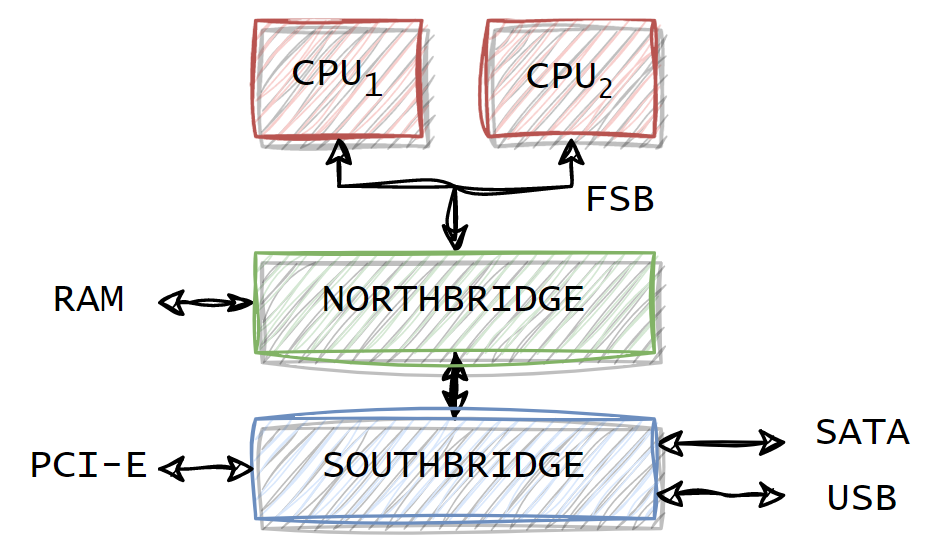
The main bottleneck in the architecture above is the Northbridge communication to the RAM. In this architecture, the northbridge contains the memory controller for interfacing with the RAM. Therefore, the data goes through a unique memory bus and a unique memory controller.
Nowadays, the architectures integrate the memory controllers into the CPU so that there is no need for the northbridge at all. Below are the schema describing an architecture without the Northbridge:
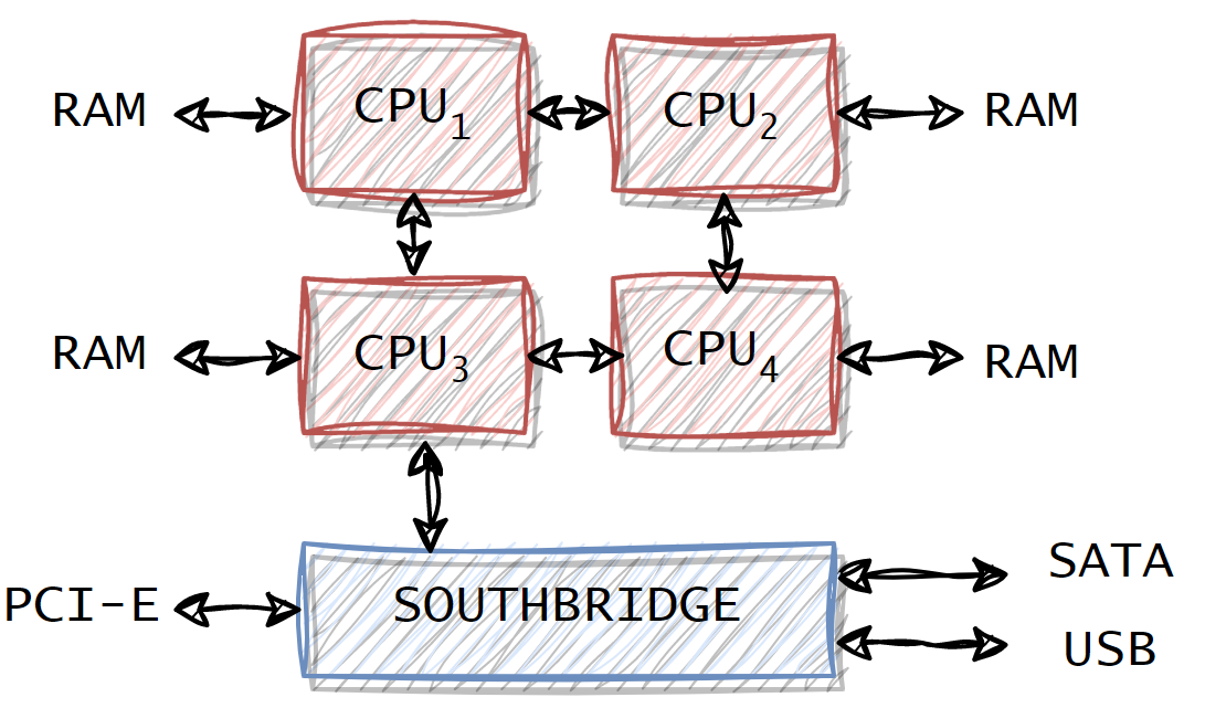
In this case, the memory bandwidth is proportional to the number of CPUs. This architecture leads to a non-uniform memory because the memory is now bounded to the CPU (local memory) usually referred to as NUMA: Non-Uniform Memory Architecture. (See dedicated section for more details.)
Optimizing device access with DMA
In the early architectures, every communication to/from a device had to pass through the CPU. This has been solved with DMA. DMA is an optimization for offloading the CPU. It allows transferring data from devices with minimal effort from the CPU only needs to initiate the transfer and move over to new tasks.
NUMA
NUMA stands for Non-uniform memory architectures. The non-uniform part refers to the locality of the memory compared with the CPU.
In a NUMA architecture, a processor can access its local memory faster than non-local memory. As already mentioned, the Non-uniform memory is needed because the northbridge becomes a severe bottleneck since all the memory traffic is routed through it. So, the memory controller and the memory are integrated into the CPU.
NUMA requires that the OS takes into account the distributed nature of the memory:
- if a process run on a given processor then the physical RAM assigned to the process address space should be from the local memory of that processor.
- the OS should not migrate a process or a thread from one node to another. In case migrating the process across nodes is necessary then the selection of the new processor should be restricted to processors that do not have higher access costs to the memory than the current processor.
The memory allocated in NUMA is by default not allocated only on the local node to avoid saturation of the local memory of nodes that are running large processes.
CPU caches
The memory is not as fast as the CPU. Thus, the need for CPU caches between CPUs and memory. It is feasible to build a faster RAM (see SRAM internals), but it is not cheap. The choice is either for a large amount of DRAM or for a smaller amount of very fast SRAM.
The approach taken on most of the commodity hardware is hybrid. The DRAM is used as the main memory facility. On top of that, there is a small amount of SRAM to cache data used in the near future by the processor.
Architecture
The CPU caches architecture consists of many cache layers. The reason for having many layers is historical. The new layers are added as the speed difference between the cache and main memory continues increasing.
Below is the schema of a 3 levels cache architecture:
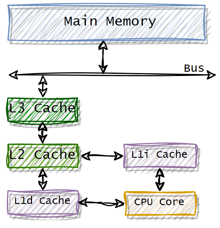
The speed is higher in the cache layers closer to the core. The architecture presents two flavours of L1 cache:
L1dcache is dedicated to the data.L1icache is dedicated to the instructions.
In a multi-processor / multi-core architecture a cache might be shared depending on the level. The paper describes the cache in a multi-processor architecture with the following schema:
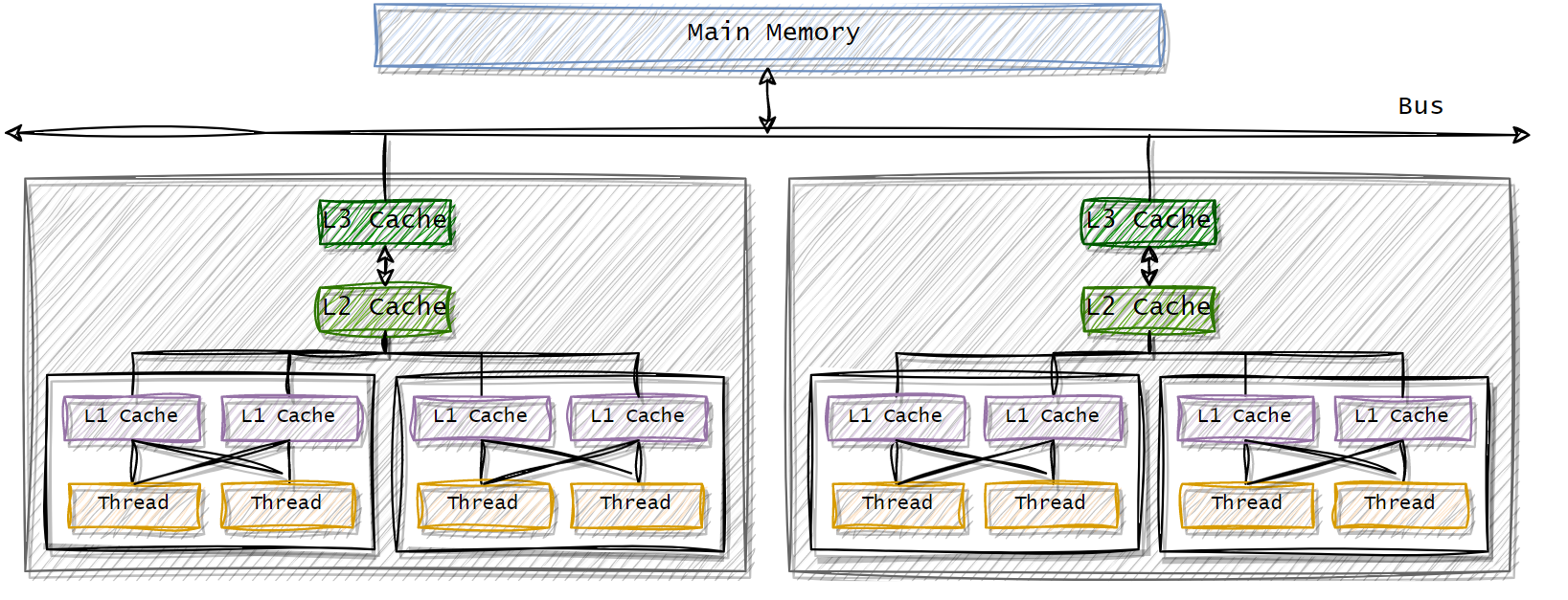
The schema represent a 2 processor, each one with 2 cores. Each core has 2 threads respectively. The L2 and L3 caches are shared across the cores within a processor, while the threads within a core shares L1 caches.
CPU caches implementation
All the data read or written by the CPU is stored in the CPU caches. If the CPU needs a data word, it searches in the caches first. Entries are stored in the cache as lines of several contiguous words for the following reasons:
- The spatial locality: in a short period, there is a good chance that the same code or data gets reused.
- The RAM modules are more effective if they can transport many data words in a row.
When the processor needs the memory content the entire cache line is loaded into the L1d. The following steps describe, at high-level, the process for modifying memory:
- The processor loads a cache line first.
- The processor modifies the interested part of the cache line, marking it as "dirty".
- When the processor writes back the changes to the main memory the dirty flag is cleared.
To load data in a cache it is necessary to make room in the cache. The eviction process from L1d pushes the cache line down into L2. In turn, evicting the cache in L2 means pushing the content into L3. Finally, L3 pushes content into the main memory.
Associativity
The core problem in CPU cache implementations is that many memory locations fight for each place in the cache. The cache associativity plays a role in the performance of the overall system. In specific, the associativity determines where a particular memory block can be placed when it is loaded into the cache.
     ┌──────────────┬────────────────────┬───────────┐
     │     TAG      │      SET INDEX     │   BLOCK   │
     │              │                    │   OFFSET  │
     └──────────────┴────────────────────┴───────────┘
          t bits            s bits           b bits
The caches are organized in sets divided into cache lines. The addresses referring to cache values are usually composed of the followings parts:
- Tag represents the tag to store alongside the cached value. The tag contains the address of the target data in the main memory. It is needed because in some cases many memory addresses can end up being stored in the same cache line, see associativity types below.
- Set index identifies the target set.
- Block offset identifies the offset within the cache line. A cache line can store many words; the offset is needed to identify a single word.
There are 3 types of CPU caches: the direct-mapped, fully-associative and set-associative types. Each of them determines how the content of the cache is stored and fetched.
Direct-mapped cache
The cache is organized into many sets with a single cache line per set. Thus, a memory block can only occupy a single cache line.
The write pattern is as simple as placing the memory block in the set index identified by the address. The tag is stored alongside the set. The new data replace the old one already stored.
The search pattern is as simple as retrieving the set corresponding to the set index contained in the address. If the tag (stored alongside the set) corresponds to the tag in the address then the data is retrieved from the cache (cache hit). Otherwise, it is a cache miss.
The advantage of this approach is that it is simple and cheap to implement. The disadvantage is that it leads to a lot of cache misses.
Fully-associative cache
A fully-associative cache is organized in a unique set with many cache lines.
A memory block can be placed in any of the cache lines. The addresses of a fully-associative cache do not have any Set index as the set is unique.
The write pattern consists in looking for the first cache line available to place the memory block. If no space is available, a block in the cache is evicted based on a replacement policy.
The search pattern consists in checking each Tag field against the memory address with the tag bits associated with each cache line. The Offset is used to select the byte to return.
The advantage is that the cache is fully utilised and the cache hits rate is maximized. The disadvantages are that the search pattern iterates over all the cache lines and the implementation is expensive.
Because of the performance and hardware costs, this approach is usually adopted for small caches with a few dozen of entries.
Set-associative
It is a hybrid between the fully associative and the direct-mapped approach. Each set can contain many cache lines. It is the go-to approach for CPU caches.
A memory block is first mapped to a set and then it can be placed into any cache line of that set.
The writing pattern consists in placing the memory block in any of the cache lines in the set defined by the Set index. The tag is stored in the field associated with the cache line. In case all the cache lines are occupied, then one block in that set is evicted.
The search pattern identifies the set using the Set index. The Tag bit is compared with the tags of all cache lines of the set.
This approach is a trade-off between the previous two approaches.
Write behaviours in a single processor
The paper describes 3 cache policy implementations to achieve coherency in a single processor scenario: write-through, write-back and write-combining.
The write-through implementation is the simplest. If the cache line is written to, the processor immediately also writes it to the main memory. This implementation is simple but not fast and it creates a lot of traffic on the FSB.
The write-back implementation consists in marking the cache line dirty just after it is updated. When the cache line is dropped from the cache the dirty bit will instruct the processor to write the data back to the main memory. The write-back approach is more complex, but it provides better performance. The write-back approach is the widespread approach adopted by the processors.
The write-combining implementation combines many write accesses before the cache line is written. This approach is used to cut the transfer and it is usually used when a device is involved, such as a GPU.
Multi-processor coherency and MESI
The cache behaviours get more complicated in a multi-processor setup. The write-back implementation fails to keep a consistent coherency with many processors.
Let's take as an example a 2 processors scenario (P1, P2). P1 writes an updated cache line, that cache line won't be available either on the main memory or on the caches of the P2, as they don't share the same caches. Thus, the P2 would read out-of-date information.
Providing access from P2 to the cache of P1 would be impractical for performance reasons. Thus, the go-to approach is to transfer the cached content over to the other processor in case it is needed. The same is also valid for the caches that are not shared on the same processor. The cache line transfer happens when a processor needs a cache line which is dirty in another processor.
The MESI is the coherency protocol that is used to implement write-back caches in a multi-processor scenario.
MESI takes the name from the 4 states a cache line can be:
- Modified: the cache line is dirty and only present in the current cache.
- Exclusive: the cache line is only present in the current cache, but it is not modified.
- Shared: the cache line is stored in many caches but is clean (it matches the main memory)
- Invalid: the cache line is invalid.
The cache lines are initialized as Invalid:
- when data is loaded into the cache for writing the cache line is marked as
Modified. - when data is loaded for reading the state depends on other processors:
- if another processor has the same data then the line is marked as
Shared - if no other processor has the same data then the line is
Exclusive
- if another processor has the same data then the line is marked as
The state of the cache line is subject 2 main stimuli:
- a local request, which does not need to notify other processors. For example, it happens when a
ModifiedorExclusivecache line is read or written locally. In this case, the state does not change. - a bus request, which happens when a processor needs to notify another processor. Some examples:
- a processor called
P2wants to read the cache line from another processorP1.P1has to send the content of the cache toP1and change the state toShared. The data is sent to the memory controller that stores the data in memory. - a processor called
P2wants to write a cache line that is in aSharedorInvalidstate. This operation would trigger a bus request to notify the other processors and mark their local copyInvalid.
- a processor called
In general, a write operation can only be performed as a local request if the cache line is in Modified / Exclusive state. In case a write-request acts on a cache line in a Shared state, then all the other cached copies must be invalidated. The invalidation process happens by notifying the change of the other processors. This is also known as Request for ownership (RFO).
Performance considerations on CPU caches
Associativity plays a crucial role in reducing cache misses, and thus in the performance of the CPU caches. The paper demonstrates how moving from direct to set associativity can reduce cache misses by the 44% in a 8M L2 cache layer.
Worth mentioning that another factor that plays a role in the cache misses reduction is the cache size. Larger the cache, less are the chances to encounter cache misses.
Request for ownership (RFO) in the context of MESI can slow down things in the context of multi-processor operations. They are expensive coordination operations. The coherency messages need to be sent to N processors and await a reply from all of them. So, the speed of this exchange is determined by the longest possible time needed to get a reply.
Virtual Memory
The paper proceeds by describing the virtual memory system used by the processors. The virtual memory provides the virtual address spaces used by the processors. Some of the advantages of virtual memory:
- Virtual memory handles the offloading of the physical memory by moving the in-memory data into a disk.
- Provides a transparent abstraction to the process. The processes see the memory as a unique chunk.
The component taking care of the virtual address space is the Memory management unit (MMU).
Address translation
The core functionality of the Memory management unit (MMU) is the translation from a virtual address to a physical address.
The translation is implemented using the multi-level page table structure. Defined in the paper with the following schema:
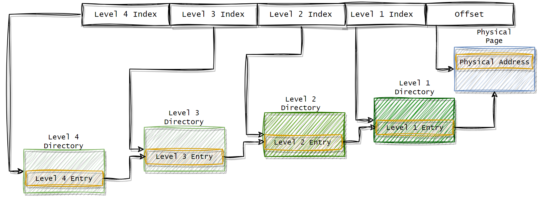
The virtual address is divided into 5 parts. The Level 4 index points to the Level 4 Entry which is a reference to the Level 3 Directory. The structure continues until the Level 1 Directory where the entry contains the reference to the physical page. The combination of the physical page address plus the offset is the physical address and the operation of recursively navigating the page table is defined as page tree walking.
The data structure for building the page table is kept in the main memory. Each process has its own page table. The CPU is notified of every creation or change of a page table. The page tree walking operation is expensive. For example, for a 4-level page tree, the operation needs at least 4 memory accesses. On top of that, the address computation cannot be parallelized because an address depends on the up-level directory.
Thus, it is necessary to precompute the mapping between the virtual address and the physical address. The pre-computed values are stored in the Transaction Look-Aside Buffer (TLB).
The Transaction Look-Aside Buffer (TLB) is usually built with a set or a fully associative approach (depending on the purpose of the architecture). If the tag has a match in the cache, the physical address is computed by adding the offset specified in the virtual address. In case of a TLB cache miss, the CPU needs to execute the page tree walking process and store the result in the TLB cache.
Note that the TLB follow the same structure as the other CPU caches, so it can have built by many layers: L1TLB, L2TLB. Futhermore, there can be many TLB for many purposes: an instruction TLB and a data TLB.
Performance considerations on TLB
TLB size is limited like for the CPU caches. The performances of TLB can be influenced by changing the size of the pages.
Larger pages reduce the number of address translations needed, meaning that fewer TLB entries are needed. Futhermore, in case of TLB miss, the page tree walk will be faster as the number of levels will be smaller.
The downside of this approach is that the large pages must be contiguous in the physical memory. This results in a more fragmented memory, and an increase in wasted memory.
Huge pages are beneficial in a scenario where performance matters and resources are not a concern. For example database servers or systems where latency matters. This series of posts provide a detailed overview on the use of huge pages:
Low Latency Optimization: Using Huge Pages on Linux (Part 1)
Low Latency Optimization: Using Huge Pages on Linux (Part 2)
Wrap-Up
This post analyzes some of the topics discussed in the paper What Every Programmer Should Know About Memory by Ulrich Drepper. CPU caches, Virtual memory, TLB and the anatomy of the hardware plays a role in optimizing the performance of the system.
The next post (Memory management optimization techniques) of this series is more hands-on and it explores the concepts introduced in the "What programmers can do" section of Ulrich's paper.
References
What Every Programmer Should Know About Memory - Ulrich Drepper
Low Latency Optimization: Using Huge Pages on Linux (Part 1)
Low Latency Optimization: Using Huge Pages on Linux (Part 2)